Solving the Transfer Challenge
for MicroLED Display and Micro Semiconductor Fabrication at Scale
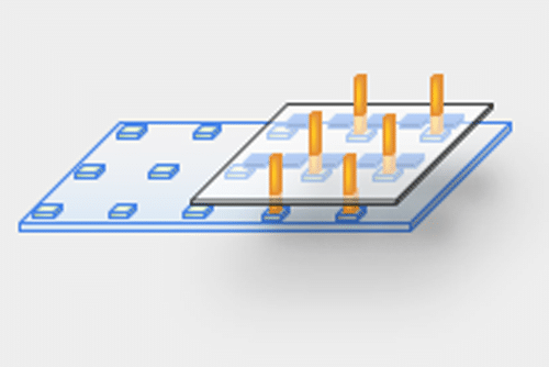
MicroSolid Printing™ Versus Laser and Pick and Place
MicroSolid Printing™ cracks the code in the efficient transfer of LEDs from wafer to backplane. With an initial focus on microLED displays, the platform will help enable a $30 billion market by 2030.The Problem:
Traditional methods like laser and pick-and-place are:Inefficient
Costly
Unscalable
Environmentally Unfriendly
The Solution:
MicroSolid Printing™: A scalable, eco-friendly turnkey approach that delivers unparalleled results over other transfer methods.Superior Performance
Exceptional visual quality and energy efficiency
Tunable transparency from 80% to zero
Versatile applications across industries
Unmatched Efficiency
99.999% yield rate
2-5 times higher throughput
Rapid placement of tens of millions of micro-LEDs
Cost-Effective Production
2-5 times more economical
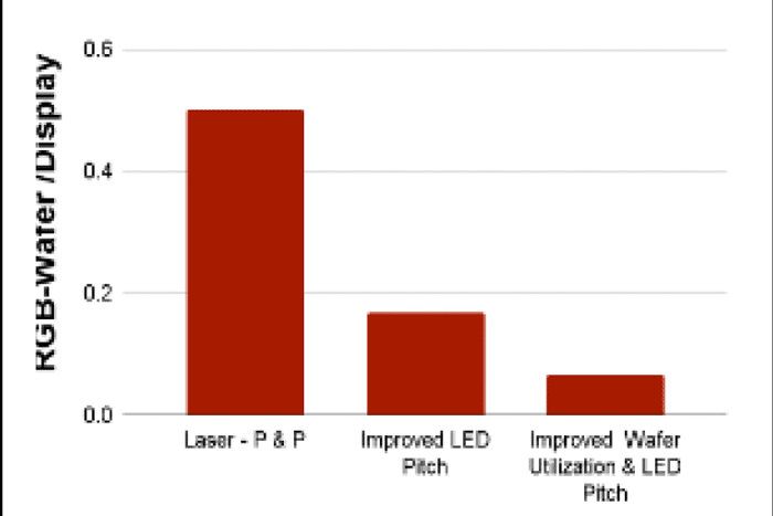
Up to 10x reduction in wafer usage
80% wafer utilization (compared to <50% for other solutions)
MicroSolid Printing™ is paving the way for widespread adoption of microLED display technology and life-changing micro semiconductor products.
Laser Release
High Selectivity
Pick & Place (P&P)
Simple Tool
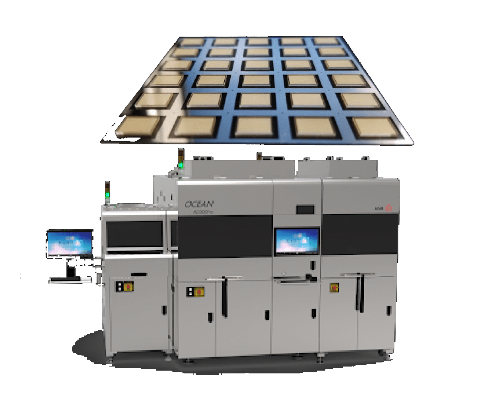
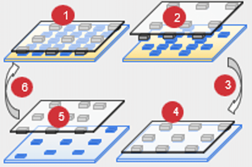
MicroSolid PRINTING™
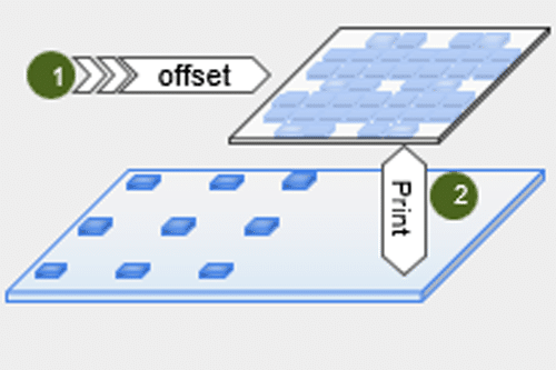
Scalable • Affordable • Uniform
MicroSolid Printing™: Unparalleled Results
MicroSolid Printing™ addresses four key obstacles in microLED and micro semiconductor fabrication:High Yield
- Achieves rapid transfer of millions of micropixel devices.
- Delivers near-perfect yield with zero defects.
Unmatched Throughput
- Efficiently transfers millions of microLED chips.
- Outperforms traditional methods like laser and pick-and-place.
Superior Performance
- Overcomes wafer non-uniformity challenges.
- Achieves >80% wafer utilization (vs. <50% for traditional solutions).
Cost-Effective Integration
- Seamlessly integrates with existing fabrication processes.
- Enables transition to microLED or micro semi devices with minimal CApEX.
MicroSolid Printing™ advances both microLED displays and micro semiconductor applications, propelling industry innovation.
Material Cost
- 2-5x lower cost
- Enabling smartphone by meeting the cost and scale
Throughput
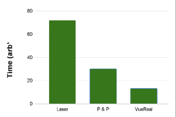
- 2x faster using similar tool
- 6x faster in our roadmap
Uniformity
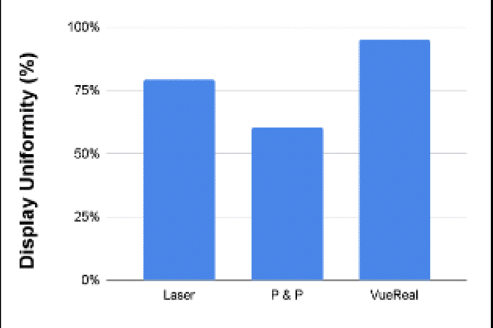
- Managing non-uniformity
- Rendering more wafers useful
Want to learn more?