Nano-/Micro-fabrication is practical and never far away from our life.
To many people, Nano-/Micro-fabrication is probably the farthest thing from their mind. Lots of times, people just see “well-armed” researchers or engineers busily walking around in an isolated room and doing nothing besides some stainless-steel chambers. Somehow, they come out and show you something cannot be seen with naked eyes and tell you how impressive the fancy stuff is. One moment, you are shocked by the invisible stuff and give them a thumbs-up. And then, you start to ask yourself silently: what the hell is that?
Nano-/Micro-fabrication is practical and never far away from our life. From laptops to smartphones, from electric vehicles to satellite, Nano-/Micro-fabrication always make things small enough to change the world. It is neither a mystical process nor an abstruse method. In my opinion, rather, it is very similar to cooking.
Both cooking and Nano-/Micro-fabrication start from raw materials to delivering well treated and organized products for consumption. There are some basic methods of cooking: roasting, frying, boiling, baking, steaming. Various methods use differing levels of heat and vary in cooking time. The method chosen greatly affects the end result because some food materials are more appropriate to some methods than others. Some complex Chinese food cooking even requires a combination of three or more methods in sort of sequence. The same thing for Nano-/Micro-fabrication, it also a combination of some basic methods: lithography (photo, electron-beam, & Nano-imprint), deposition, etching (dry & wet), polishing, bonding. Micro-LED device fabrication, for example, needs to perform over 20 major steps including multiple lithography processes repeatedly and various deposition and etching one after another to build up the entire structure and make a device working efficiently.
Unlike machining manufacturer, which works directly on a bulk material, Nano-/Micro-fabrication usually starts on top a thick support substrate called wafer (Si, GaAs, quartz, etc.). All the fabrication steps happen layer by layer on the wafer, which also enables easy handling of the device. This is quite similar to making sushi rolls. The bamboo mat works as the substrate. You place a sheet of seaweed on top of the bamboo mat and then spread a thin layer of rice, a layer of salmon, and other ingredients. Roll the sushi up from the bottom using the bamboo mat and then cut it into smaller rolls. In our micro-LED device fabrication, we also fabricate many individual devices together on a piece of wafer and separate them at the end of fabrication.
Just like making various cookies shapes, we want to customize our device size and structures as well. Since we cannot sculpture or mold our device in Nano-/Micro-fabrication processes, the only way to pattern distinct features for deposition and etching steps is to use lithography. Photolithography is usually used to define micrometre scale features. While electron-beam lithography does a good job in nanometre scale patterning. For mass production, Nano-imprint lithography is preferable. It works as making waffles. The pre-designed and pre-heated waffle irons make the liquid waffle mixture golden and crispy. The “mixture” for the Nano-imprint lithography is called resist. By applying certain temperature and force, the resist is patterned and hardened as designed for later steps.
Another similarity between cooking and Nano-/Micro-fabrication is they both need “recipes” to process. The “recipe” requires accurate temperature, pressure, and timing control. They can either give you a tender and juicy steak or heavily burnt wings. They can also give me accurate etching rate or a bad quality dielectric thin film for my device. In Nano-/Micro-fabrication, even a small temperature variation or bad timing would cause device failure. Therefore, a good recipe is able to protect previously fabricated structures/materials and build up new ones. Imaging you stew your beef and potato for the same amount of time. However, if you develop perfect recipes, congratulations: deposition and etching are as easy as you are putting your seasoned turkey into the oven.
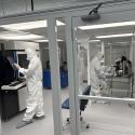
As a Nano-/Micro-fabrication researcher, my “kitchen” is called cleanroom. It is designed to maintain extremely low levels of particulates, such as dust, airborne organisms, or vaporized particles. At a micrometre scale, a small piece of dust is like a “huge rock” for the devices. Thus, the cleanness of our “kitchen” guarantees good health and mood for our customers as well. Nevertheless, a cleanroom is not that easily built as a Kitchen in terms of cost, precision instruments, and maintenance. Lots of companies demanding Nano-/Micro-fabrication must share the facilities with other company in Universities or other institutions. VueReal is now building our own cleanroom for our “chefs”. With our own “Kitchen”, our professional “chefs” are more concentrated and dedicated to pushing out new “dishes and cuisine” of micro-LEDs to make your life tasty and colourful.
Nano-/Micro-fabrication is never far from you. The wonderful world in the big display will be brought to you by the invisible micro-LED devices from VueReal.


